Hardware Simulation using Open Source tools: a case study using nand2Tetris
Ever since I joined AMD, I developed a deeper appreciation for hardware and this has translated in a desire to understand better how computers work at the lowest level. Last year I started a wonderful course called nand2Tetris: bulding a modern computer from first principles. I had a lot of fun going through Part I, and while the Hardware Description Language used in the class was clear and simple, I wanted to challenge my knowledge using the industry standard SystemVerilog and emulating the full computer using only Open Source Software (C++ and verilator). In this post I will walk through my learning process, from the basics of the computer to its full simulation.
Hack Computer Architecture
The nand2Tetris computer is called HACK and is based on a modified von Neumann Architercure. In a classical von Neumann architecture the memory is shared between the program and the data memory. The HACK computer splits the memory in two separate banks, one for read only part for the program (ROM), and a random access memory (RAM) for the data.
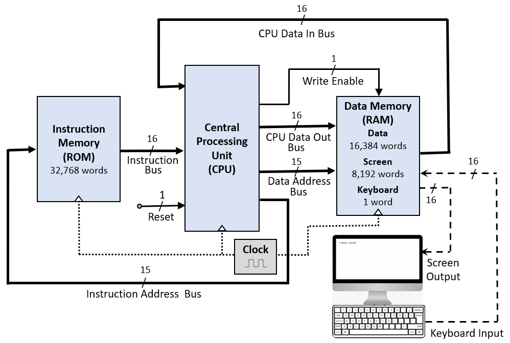 Hack Computer Architecture. By Rleininger - Own work, CC BY-SA 4.0, https://commons.wikimedia.org/w/index.php?curid=109499961
The architecture consists of three key components:
CPU: Features a minimalistic design with an Arithmetic Logic Unit (ALU) and two main registers: A (address or value) and D (data). The CPU executes one instruction per clock cycle, which drives the pace of computation. Each cycle processes an instruction—fetching it from memory, decoding it, executing it, and writing back results—all within a single tick of the clock.
Memory: Includes 32K words of RAM for data, along with memory-mapped I/O for a screen and keyboard. Programs are stored in ROM.
I/O: The screen and keyboard are accessed via specific memory addresses, allowing interaction without dedicated instructions.
The instruction set is deliberately minimal: just A-instructions for setting memory addresses or constants, and C-instructions for performing computations, memory access, and jumps. This simplicity makes Hack an ideal model for learning how hardware executes software at the machine level.
In the Hack computer architecture, the CPU executes one instruction per clock cycle. The system is synchronous, meaning that all state changes—such as writing to registers or memory—occur on the positive edge of the clock signal (when the clock transitions from low to high).
Importantly, the clock cycle begins at the negative edge of the clock. This design allows the combinational logic within the CPU to stabilize before the next state is latched at the positive edge. Here’s a breakdown of what happens during each cycle:
- Start of Cycle (Negative Edge)
- No state is updated yet; this phase begins the cycle.
- The Program Counter (PC) outputs an address to the instruction memory (ROM).
- The ROM returns the instruction at that address.
- The instruction is decoded and fed through combinational logic.
- If it is an A-instruction, the 15-bit constant is prepared for loading into the A register.
- If it is a C-instruction, the ALU computes the result based on the current values of the A or RAM[A] and D registers.
- The destination is evaluated and enabling signals are sent to the respective AMD destinations.
- The jump condition is also evaluated combinationally to determine the next PC value.
End of Cycle (Positive Edge)
- At the rising edge of the clock, all enabled state elements are updated simultaneously:
- The A register is loaded either with the constant from an A-instruction or with the ALU output if specified in a C-instruction.
- The D register is updated with the ALU result if the destination bits include D.
- The RAM is written to if the instruction specifies memory output (via M) and uses the address in the A register.
- The Program Counter is either incremented (by default) or updated with the value in the A register if a jump condition is met.
It helps to look at these cycles with an example. Let’s consider this Hack assembly code:
(END)
@END
0;JMP
These instructions create an infinite loop, and are used at the end of every Hack program. Assuming that the PC was at value 100, when hitting the @END.
| Cycle | Phase | PC | A | Instruction | Action Taken at negedge |
|---|---|---|---|---|---|
| 1 | negedge | 42 | ?? | @END | Decode A-instr → Prepare to set A = 42, PC + 1 |
| 2 | negedge | 43 | 42 | 0;JMP | comp = 0, jump = JMP → Next PC = A = 42 |
| 3 | negedge | 42 | 42 | @END | Decode A-instr → Prepare to set A = 42, PC + 1 |
| 4 | negedge | 43 | 42 | 0;JMP | comp = 0, jump = JMP → Next PC = A = 42 |
One importance difference to point out between hardware and software can be drawn by looking at the A instructions. In software one might optimize the code without activating the ALU of the CPU, while in hardware the ALU is always active regardless of the instruction.
Describing hardware using SystemVerilog
Now that we’ve explored the Hack CPU’s hardware design — including how instructions flow through the ALU, control logic, and registers — the next natural step is to move from diagrams to actual implementation.
This is where SystemVerilog comes in: a modern hardware description language (HDL) that lets us describe, simulate, and synthesize digital circuits like the Hack CPU.
In the Hack CPU, both the D and A registers are 16-bit state elements that update on the rising edge of the clock when a control signal (load) is high. Using your parameterized Register module, we can instantiate these registers cleanly and reuse the same code for both.
The code for the Register could be written as:
1
2
3
4
5
6
7
8
9
10
11
12
13
14
15
16
17
18
19
20
21
22
module Register #(parameter WIDTH = 16)(
    input logic clk,
    input logic load,
    input logic  [WIDTH - 1 : 0]  in,
    output logic [WIDTH - 1 : 0] out
);

logic [WIDTH - 1 : 0] memory;

initial begin
    memory = WIDTH'(0);
end

always_ff @(posedge clk) begin
    if (load) begin
        memory <= in;
    end
end

assign out = memory;

endmodule
The code above describes a parametrized SystemVerilog module where an internal memory is initialized as 0. Subsequently on the positive edge of a clock signal the input signal is assigned to the memory if the load signal is asserted. Finally a combinatinal logic block assign the memory to the output signal.
All the pieces of the architecture can be described using this language, and my implementation can be found in the hack_emu repo.
Testing SystemVerilog Code
Once a module is written is always good to test in isolation using a testbench. I have written those using a technique named self checking testbench from the Digital Design and Computer Architecture book from Harris and Harris.
This approach lets the user write a SystemVerilog file where an instance of the module under test (generally name device under test - dut), gets inputs assigned from a file and then the outputs from dut are compared against the expected values.
The different phases can be resumed as follow:
- Instantiate the Device Under Test
1
2
3
4
5
6
7
 // Instantiate the module under test (DUT)
  Register dut (
    .clk(clk),
    .in(in),
    .load(load),
    .out(out)
  );
- Read and initialize the input and expected output from file. Also write simulation file (vcd) on disk
1
2
3
4
5
6
7
   initial begin
    clk = 1;
    in = 16'b0;load = 0; out_exp=16'b0;
    $dumpfile("Register.vcd");
    $readmemb("../tb/Register.tv", testvectors, 0, 147);
    vectornum = 0; errors = 0; testnum = 0;
  end
- Assign the inputs, and the expected output
1
2
3
4
5
6
7
8
9
10
    #4; // Do not have inputs changing right on clock edge
    load = testvectors[vectornum][16];
    in = testvectors[vectornum][32:17];
    #1;
    clk = ~clk; // 10ns clock period (5ns high, 5ns low)
    out_exp = testvectors[vectornum][15:0];
    if (testvectors[vectornum] === 33'bx) begin
      $display("%d tests completed with %d errors", vectornum, errors);
      $finish;
    end
- Check the outputs and report errors
1
2
3
4
5
6
7
8
9
10
11
 #1; // Artificial Delay to let the DUT run.
    if (out !== out_exp) begin
      $display ("Test: %d", {testnum});
      $display ("CLK: %b", {clk});

      $display("Error: inputs = %b", {in, load} );
      $display("  ouputs = %b (%b expected)", out, out_exp);
      errors = errors + 1;
    end
    vectornum = vectornum + 1;
    testnum = testnum + 1;
I found that in simulation is very important to not let signals change and check for results right on the clock edge, rather allow some delay and check later.
The test files like Register.tv mentioned above are translated in binary from the verification files provided from Nand2Tetris, to convince myself that I was simulating exactly the same design. One challenge I found is that for sequential logic the original verification files provide the state of a register as well on a posedge, however in this state we are committing data to memory, so I decided to check only output of sequential logic on negedge. This does not apply to ALU, as it is a combinational circuit.
To run the tests I have used icarus verilog and vvp, together with GTKWave to manually check the results, and the documentation with a simple example can be found here.
Simulating the Computer using Verilator
The testbenches discussed earlier function essentially as unit tests for individual components of the architecture, as they evaluate parts in isolation rather than as an integrated system. To move beyond this and simulate the entire computer—from ROM, through the CPU, and into main memory, including peripherals like the screen and keyboard—I turned to Verilator. Verilator is an open-source tool that translates SystemVerilog modules into a high-performance C++ library, making it ideal for this kind of system-level simulation.
What makes this approach especially compelling is its flexibility: by converting SystemVerilog files into a C++ dynamic library, developers can embed their hardware models directly into a native C++ application. This allows for realistic simulation of I/O devices like screens and keyboards, providing an interactive environment for system testing.
To manage the build process, I used CMake both to compile the Verilated library and to link it with a C++ executable that drives the simulation. This C++ code implements a full-system simulation of the HACK computer, combining a Verilated hardware model with SDL2 for real-time screen output and keyboard input. The simulation starts by initializing Verilator and the HACK CPU model (VComputer), followed by loading a .hack binary program into the simulated ROM. The loadProgram function parses a text-based binary file line by line, converting each 16-bit instruction into a format suitable for directly populating the ROM memory in the Verilated model.
1
2
3
4
5
6
7
8
9
10
11
12
13
14
15
16
17
18
19
20
21
22
23
24
25
26
27
28
29
30
31
32
33
// Load a HACK program into ROM
bool loadProgram(VComputer* top, const std::string& filename) {
    std::ifstream file(filename);
    if (!file.is_open()) {
        std::cerr << "Error: Could not open program file " << filename << std::endl;
        return false;
    }

    std::string line;
    int address = 0;

    std::cout << "Loading program " << filename << "..." << std::endl;

    while (std::getline(file, line) && address < ROM_SIZE) {
        // Ignore empty lines and comments
        if (line.empty() || line[0] == '/') continue;

        // Check if it's a binary string (16 characters of 0s and 1s)
        if (line.length() >= 16) {
            uint16_t instruction = 0;
            for (int i = 0; i < 16; i++) {
                if (line[i] == '1') {
                    instruction |= (1 << (15-i));
                }
            }

            // Set instruction in ROM
            // Note: Adjust this based on your actual module interface
            top->Computer->rom->rom[address] = instruction;
            address++;
        }
    }
What is interesting in the snippet above is how using Verilator the programmer can directly poke the ROM values.
Next, the program initializes SDL2, which is responsible for creating a window and rendering the simulated screen. SDL is set up with a window, renderer, and texture buffer that mimics the 512x256 screen resolution of the HACK computer. A pixel buffer is allocated in memory to store screen data, and a simulation loop begins. This loop cycles the hardware clock, checks for SDL events (such as keyboard or window close actions), and periodically updates the screen display from memory-mapped screen data, mimicking real hardware behavior.
The updateScreen function reads from the screen_out memory array in the Verilated HACK model. Each 16-bit word represents 16 horizontal pixels. The code interprets each bit in these words as either black (on) or white (off) and writes the corresponding ARGB color value into the SDL pixel buffer. This effectively mirrors how the HACK architecture maps video memory to screen output, giving a functional graphical output from the simulated hardware.
Finally, the handleKeyboard function maps SDL key events to HACK key codes, updating the keyboard input register of the Verilated model accordingly. It includes special mappings for non-ASCII keys (like arrow keys or function keys) and passes regular ASCII codes directly. When keys are released, the memory location is cleared to zero, maintaining consistent behavior. Together, these elements allow the entire system—from CPU to screen and keyboard—to be simulated as an interactive, self-contained environment.
In this simulation, the clock stepping strategy is implemented manually to mimic the real hardware clock behavior. Each iteration of the main loop toggles the clk signal of the Verilated model—first setting it to 0, calling eval() to compute combinational logic and state transitions, and then setting it to 1 followed by another eval() call. This simulates a full clock cycle, as Verilator does not manage clocking internally; it expects the user to drive clock edges explicitly. This fine-grained control is essential for ensuring deterministic behavior and accurate timing within the simulated hardware environment.
This manual approach offers flexibility to precisely control when screen updates and I/O interactions occur in relation to the CPU’s execution. In this case, the screen is updated every 1,000 cycles (SCREEN_UPDATE_INTERVAL), a performance-conscious choice that balances simulation speed with responsiveness in the SDL display. While Verilator can run at high simulation speed, this design adds throttling and visualization without distorting the logic simulation itself.
Results
With the strategy above I was able to simulate all the programs I tried for the platform including Pong. The framerate is quite low and I think this is all down to the many levels of indirection, but it is functional.
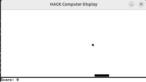 Pong running on my Simulator
Conclusions and further work
I had a lot of fun with this project and I am looking forard to load this design on an FPGA and create a software emulator.